
PCB (Printed Circuit Board), also known as printed wiring board, is a crucial electronic component serving as the support and electrical connection carrier for electronic devices. Fabricated through electronic printing techniques, it is aptly named the "printed" circuit board.
Function
The adoption of PCBs in electronic devices ensures consistency among similar boards, thereby eliminating errors in manual wiring. It enables automatic insertion or placement of electronic components, automatic soldering, and automatic testing. This guarantees the quality of electronic devices, enhances labor productivity, reduces costs, and facilitates maintenance.
Classification
1. Single-Sided Boards
On the most basic PCB, components are concentrated on one side, while conductors are concentrated on the other (with surface-mount components, they share the same side with conductors, while through-hole components are on the other side).
2. Double-Sided Boards
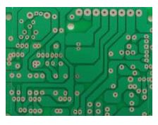
Both sides of this type of board have wiring. However, to use conductors on both sides, proper circuit connections between the two sides are necessary.
.jpeg)
3. Multi-Layer Boards
Multi-layer boards utilize more single-sided or double-sided wiring boards to increase the wiring area.
.jpeg)
PCB Heat Dissipation Methods
Electronic devices generate heat during operation, causing the internal temperature to rise rapidly. If the heat is not dissipated promptly, the device temperature will continue to rise, leading to component failure due to overheating and reduced electronic device reliability. Therefore, effective heat dissipation for PCBs is crucial. Let's discuss some PCB heat dissipation techniques.
1. Heat Dissipation Through the PCB Itself
Currently, widely used PCB materials include copper-clad/epoxy glass fabric substrates or phenolic resin glass fabric substrates, with a smaller amount of paper-based copper-clad materials.
Although these substrates have excellent electrical and processing properties, they have poor thermal conductivity. As a heat dissipation path for high-heat-generating components, little heat can be expected to be conducted through the PCB's resin itself. Instead, heat is dissipated from the component's surface into the surrounding air. However, with the trend of miniaturization, high-density installation, and high-heat generation in electronic products, relying solely on the small surface area of components for heat dissipation is insufficient. Additionally, the widespread use of surface-mount components such as QFP and BGA transfers significant heat to the PCB. Therefore, the best way to address heat dissipation is to enhance the PCB's heat dissipation capacity directly in contact with heat-generating components, conducting or radiating heat through the PCB.
▼ Adding heat-dissipating copper foil and using large-area power and ground copper foil
.jpeg)
2. Adding Heat Sinks and Thermal Conduction Plates for High-Heat-Generating Components
When a few components on the PCB generate significant heat (less than 3), heat sinks or heat pipes can be added to the heat-generating components. If temperatures remain high, fans can be integrated into the heat sinks to enhance cooling.
When numerous heat-generating components are present (more than 3), a large heat shroud (plate) can be used, custom-made according to the positions and heights of the heat-generating components on the PCB or with cutouts for different component heights on a large flat heat sink. The heat shroud fits over the components, making contact with each one for heat dissipation. However, due to inconsistencies in component heights during soldering, heat dissipation may not be effective. Flexible thermal phase change pads are often added to the component surface to improve heat dissipation.
3. Orientation of ICs for Free Convection Cooling
For devices cooled by free convection air, it is best to arrange integrated circuits (or other components) in a vertical or horizontal orientation.
4. Reasonable Wiring Design for Heat Dissipation
Due to the poor thermal conductivity of the resin in the board, while copper foil traces and holes are good conductors of heat, improving copper foil yield and increasing thermal vias are primary means of heat dissipation. Evaluating a PCB's heat dissipation capability involves calculating the equivalent thermal conductivity (θeq) of the composite material comprising various materials with different thermal conductivities, used for PCB insulating substrates.
.jpeg)
5. Zoning Components Based on Heat Generation and Dissipation
Components on the same PCB should be arranged according to their heat generation and dissipation capabilities. Components with low heat generation or poor heat resistance (e.g., small-signal transistors, small-scale integrated circuits, electrolytic capacitors) should be placed at the upstream (entrance) of the cooling airflow, while those with high heat generation or good heat resistance (e.g., power transistors, large-scale integrated circuits) should be placed downstream.
6. Component Placement for Optimal Heat Dissipation
In the horizontal direction, high-power components should be placed near the edges of the PCB to shorten the heat transfer path. In the vertical direction, they should be placed near the top of the PCB to minimize their impact on the temperatures of other components during operation.
7. Airflow for Heat Dissipation
Heat dissipation of PCBs within devices primarily relies on airflow. Therefore, when designing, it is crucial to study airflow paths and configure components or printed circuit boards (PCBs) appropriately.
Airflow tends to move towards areas of least resistance. Thus, when placing components on a PCB, avoid leaving large empty spaces in any area. The same consideration applies to the configuration of multiple PCBs within a complete device.
8. Temperature-Sensitive Components Placement
Components sensitive to temperature should be placed in the coolest areas (e.g., the bottom of the device). Avoid placing them directly above heat-generating components. Multiple components should be staggered horizontally.
9. Optimal Placement for High-Power Components
Arrange components with the highest power consumption and heat generation near optimal cooling locations. Do not place high-heat-generating components in the corners or edges of the PCB unless cooling devices are nearby. When designing power resistors, choose larger components and ensure adequate cooling space during PCB layout adjustment.
10. Uniform Power Distribution
Avoid hotspots on the PCB by distributing power uniformly across the board to maintain consistent surface temperature performance. Achieving strict uniformity can be challenging during design, but it is essential to avoid areas with too high power densities to prevent hotspots from affecting the entire circuit's operation.
If possible, thermal performance analysis of PCBs is beneficial. Some professional PCB design software now includes thermal performance analysis modules to help designers optimize circuit designs.


